Experimenting with Electronics
Since the summer of 2024, I have closely collaborated with my physical computing professor, Prayag Inchangimath. He introduced me to the fascinating world of PCBs and robotics through various projects, such as fabricating PCBs from copper boards using both ferric chloride etching and CNC machines. This entire process has been an incredible learning experience and has significantly deepened my understanding of electronic design and manufacturing. I have gained hands-on experience with various techniques and tools, developed problem-solving skills, and fostered a passion for innovation in electronics. This journey has enhanced my technical abilities and inspired me to pursue further studies and a career in this exciting field.
July, 2024 - Current
Making custom PCBs for 3D printers
Students at OCAD University can use 3D printers to create models for their classes. Previously, students had to weigh their builds for the university to charge for the filament and printing time. However, this changed when we decided to develop custom PCBs to accurately calculate the time and filament used by the 3D printers, thereby saving time and ensuring precise billing for students.
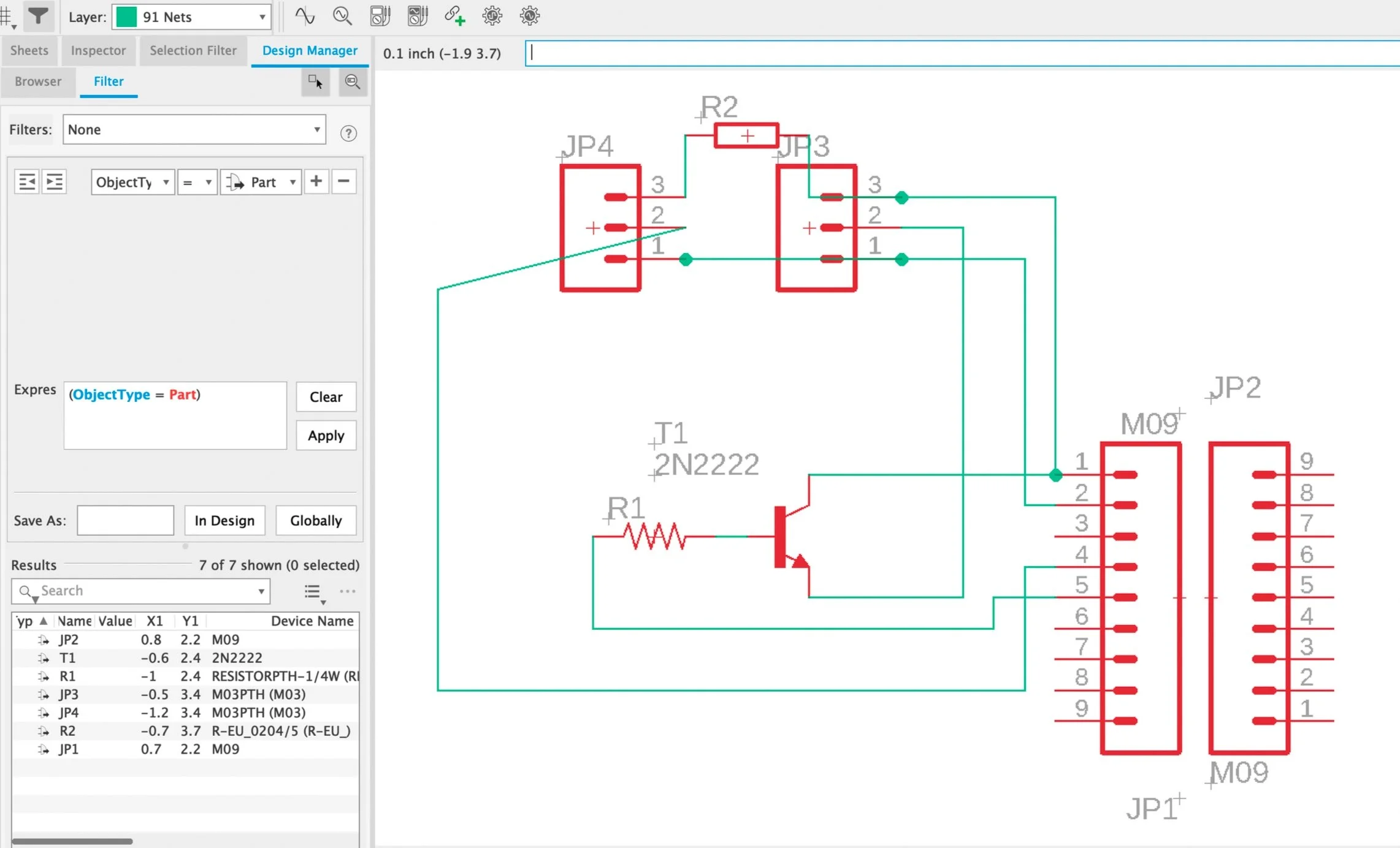
I was assigned this task and began by designing the schematic in AutoCAD EAGLE, as shown in the picture on the right. I then converted the schematic to a board layout and used the provided measurements to fit all the components onto the printer’s surface. The resulting board design is displayed in the picture at the bottom.

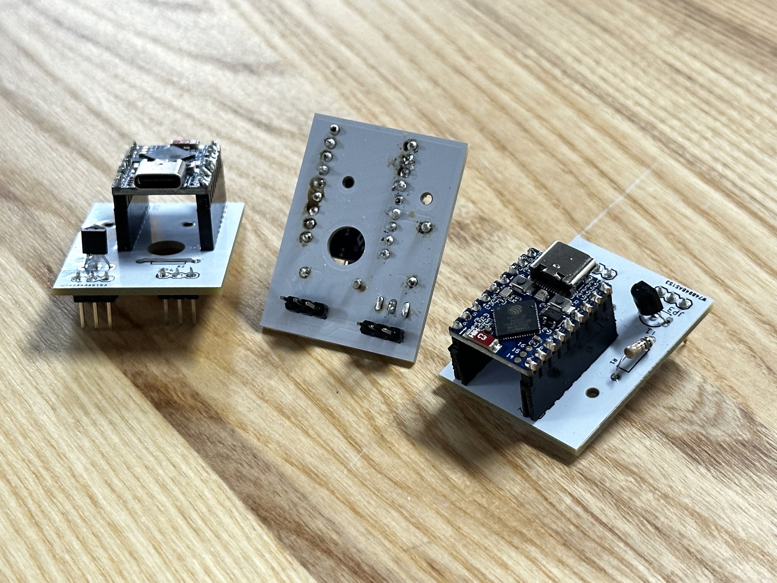
Once the PCB design was completed, we sent the files to Waveshare, who delivered the boards within a week or two. The next step was to solder all the components onto the boards. This was my first experience with soldering, and the final product is shown at the bottom.
During this project, I learned how to design PCB schematics and layouts using AutoCAD EAGLE, convert schematics into board designs, and consider component placement and board dimensions. I also gained experience in sending PCB designs to manufacturing services like Waveshare and managing the timeline for receiving the fabricated boards. I developed soldering skills by assembling the components onto the PCB, which was a hands-on and practical learning experience. Additionally, I enhanced my problem-solving skills by finding a solution to accurately measure filament and printing time, leading to the development of custom PCBs. Finally, I improved my technical documentation and communication skills throughout this project.”